
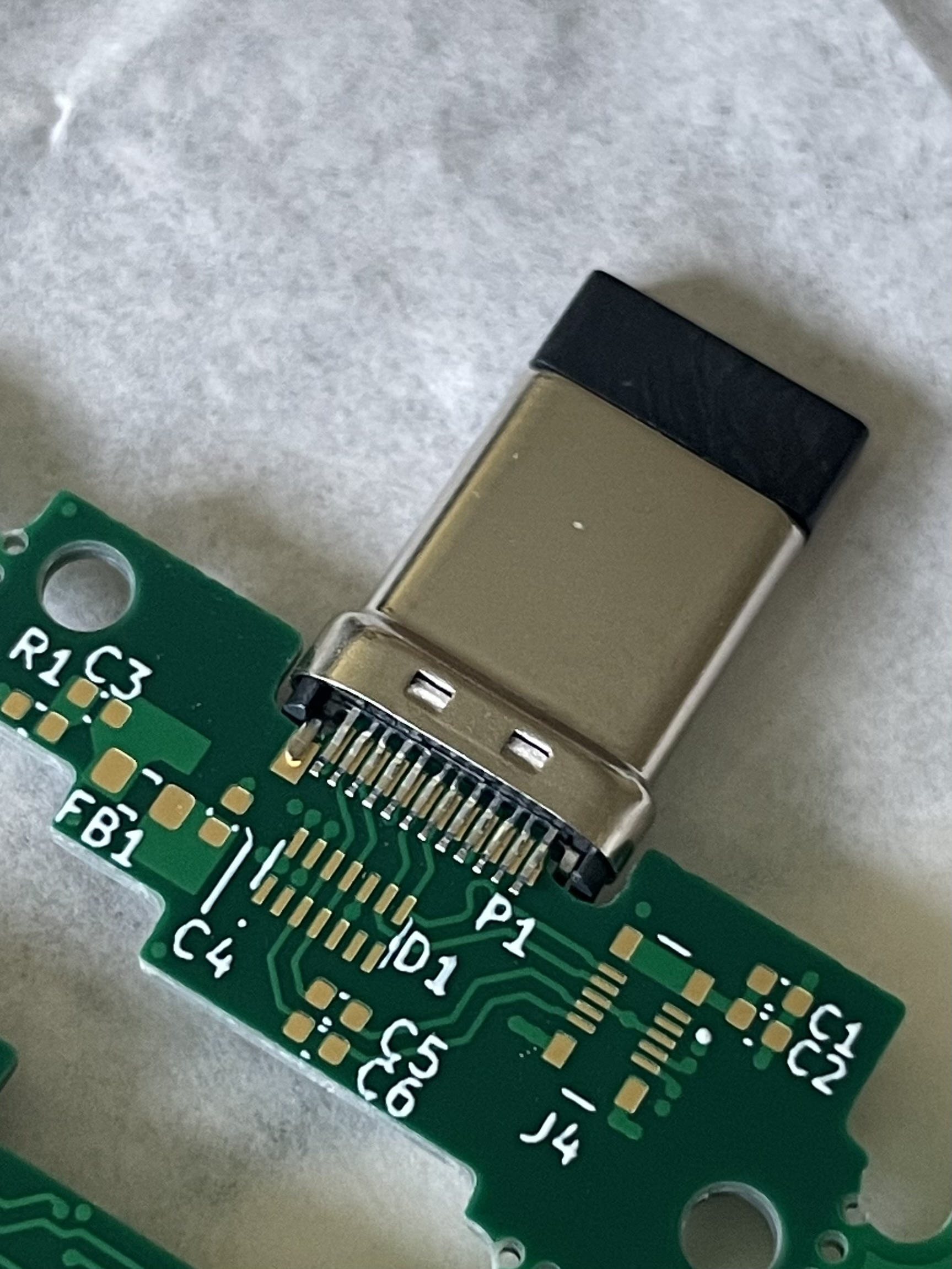
Hello :). I have some of these Molex 1054440011 USB-C edge connectors/plugs of that I somehow don’t know what’s the best way to assemble them onto my PCB.
I have the pads (standard layout from the datasheet drawing) exposed on the stencil but the pins push the paste away a little so I had quite an amount of solder bridges to rework after reflowing them. Could probably a little less solder paste (so smaller openings) and/or differently shaped stencil openings help? Also there are pins (and other components) on the backside so it’s difficult to apply paste accurately on both sides. The pins are additionally a little weirdly shaped (they bend upwards at the ends so it’s easier to push the PCB between the pins) what makes them less accessible with a soldering iron and the 0.5mm pitch doesn’t make things easier. At least the tension of the pins holds the connector in place while reflowing.
This specific one will primarily only be a one (or two)-off prototype board so I could life with some reworking but maybe someone around here has experience with these things. I also wondered how something like that would be assembled in a larger scale, the pins hold the PCB quite tight between them, I can’t imagine a pick-and-place machine could handle that.
Thanks for reading this post and maybe you have some answers :).
Not a massive fan of surface mount only USB connectors, I’d always use through hole, or at least make sure the case has a through hole mount but needs must…
If you’re not capable of soldering stuff with that pitch, and it’s nothing to be ashamed of because most people can’t, then drag soldering is the way to go.
Solder has very strong surface tension forces, when very fluid. So, if there is lots of flux gel present between the pads, and the bridge is broken only momentarily, the solder will draw back to create the minimum surface area on each of the pads. It’s almost unbelievable to see, when it happens.
Almost all of my small workshop hand tools are stainless steel medical ones - the local Government Surplus Depot sold off warship’s “First Lieutenant’s Surgery Kit” and I bought one. Then went and got another one. They have this scraper tool that just needs to be drawn across the solder bridge and the solder snaps back to the pads.
It does need the area to be flooded with zero residue flux, though. Which both helps the solder to be really, really runny and follows the tool, so that the gaps are filled with flux.
Look up “drag soldering” on YouTube. That might be your best bet. Use a chisel tip for the soldering iron and lots of flux, which you can clean up after
Thanks for your tips everyone! Here’s the complete double sided practice-board:

It’s also the first time I tried double sided reflow, which worked nicely. I did somehow expect things to fall off but they were held in place nicely. I did the side with the larger amount of components first because there are less heavy items, reflowed it, flipped it over, populated the backside and reflowed again. The only thing I didn’t think about is that I couldn’t just use the stencil easily because of the now uneven bottom side, so I just applied the solder paste with a small needle on the syringe since there weren’t too many pads. At the end I assembled the USB connector using the tips you gave here (thanks!). I’m using a cheap (slightly modified) T962 oven and lead-free solder paste for the reflow process.
It’s by the way a simple two layer reference design from framework computer for their expansion card system.